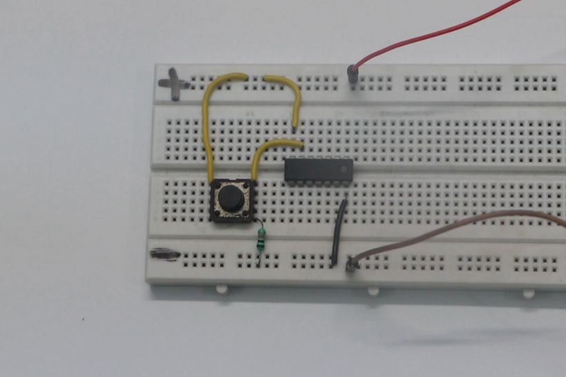
Circuit designing on a printed circuit board (PCB) is a lot easier than it may seem initially to a beginner. This ease of design is, of course, only a valid point if the project itself is not very complex. That in fact is our very first tip for beginners; do not try and undertake a project that’s overly complicated. Complicated projects can be handled later on, when you have a clear and proper understanding of the basics. So, without further delay, let’s discuss a few good practices for circuit designing that will help flatten the learning curve a bit.
Turn on Snap-to-Grid
Whatever CAD software you use, ensure that the snap-to-grid option has been turned on (0.050″ is the most widely applicable value), before placing the components in their respective places. This creates a magnetic effect on the board, which in turn helps in reducing mistakes while laying down components.
External Before Internal
Component placement is tricky, so one of the basic rules is to always place your external components on the board first, before moving on to the internal components. Examples of external components that should be put first on the PCB include:
• Mounting holes
• Switches
• Connectors
• Heat sinks
• LED lights and indicators
Use Common Mode Chokes as Unwanted Noise Filters
Common mode chokes are filters for high frequency interreferences which simultaneously:
• Block high-frequency noise interference from radio signals, inverters, motors and poorly shielded electronic equipment
• Allow pre-calibrated, low-frequency signals to pass through
Check out the common mode chokes on Octopart, and carefully select the filters you need for your particular PCB designing project. They have a huge collection from only the best manufacturers such as KEMET, TDK and Schaffner.
Functional Grouping
Functional grouping is a system of grouping components relatively close together on the circuit board, based on their core function. To be more precise, power, analog and digital components of a circuit board should not be mixed together in random. With functional grouping, it’s a lot easier to map the return path on your PCB.
Connectives Grouping
This is another method of grouping components on the PCB, but this one is based on each component’s need to connect with the other. By intelligently grouping connective components close together, you can minimize the trace lengths significantly. Minimizing trace lengths is always a sign of good circuit board design. In most cases, the connective grouping method should not clash with the functional grouping method.
Keep the Heat Dissipation Paths Clear
If the circuit board is going to generate a good amount of heat, then you will need to add dissipation vias for proper heat release. The heat release path must be kept clear by not placing any components in close proximity to the vias. In fact, this is a golden rule of PCB designing which applies to other devices such as the power op-amp as well. You do not want any of your other components to be near a high-powered component or vias, meant to dissipate excess heat generated.
Surface Mounts Over Through-Holes
Through-hole components take up a lot more space than modern surface mountable components, so you should only be using through-hole components if you do not have another choice. Another tip for saving space on your printed circuit board is to opt for ball grid components over QFP components. If you are wondering why all that space is necessary, then that’s because you will come to appreciate the extra space immensely when it is time to route the traces.
Smaller Components Should be Carefully Selected
Smaller components always seem preferable while designing the PCB, since they save so much space on the board, making it easy to route the traces. However, you should only be selecting small form factors for components, that are the least likely to require manual repairs. The smaller a component is, the more difficult it becomes to repair it manually.
Use Rotation to Shorten the Trace Lengths
As already discussed, shorter traces generate less heat and make the PCB design less complicated. However, young circuit board designers are often surprised by how much more length they can save on their trace lengths by simply rotating their components. Always rotate your components and see if the two ICs which need to be connected to each other cannot be brought closer to each other. In case you are thinking about layering instead of rotating, then that is an alternative for sure, but one which might complicate the whole routing system unnecessarily, when all it needed was a few intelligent, component rotations.
Aside from these few tips, we also have a suggestion for young PCB designers. You should be using multi-layered PCBs whenever possible. They are more costly, but almost every modern circuit board has at the very least, 4-layers. Going below that can cost your design stability in terms of power supply, and the ground plane may not be sufficient. For rudimentary designs with minimal power requirements though, a double-layer circuit board should be enough.


